
Quantum mechanics from theory to technology
It is a popular assumption that the macrophysical world is governed by classical, deterministic physics – while the microphysical world is governed by modern physics which is of statistical nature. For everyday phenomenons, it should therefore be sufficient with a basic understanding of classical mechanics, while the quantum mechanical issues may be left to the particularly interested ones. This is, however, only partly true. Fundamental everyday issues like heat conduction and heat capacity are classically incomprehensible – and even microelectronics engineering issues has started to require in-depth understanding of quantum mechanics, due to ever-shrinking feature sizes and new technologies taking advantage of quantum mechanical effects. This article gives a basic introduction into quantum mechanics and presents a few of the microelectronics technologies which take advantage of quantum mechanical effects.
Understanding quantum mechanics may be difficult, especially due to its counter-intuitive nature. From everyday life, we are used to phenomenons occurring predictably, in a deterministic and not in a statistical way. The famous quotation of Albert Einstein, “God does not play with dice”, refers to his unwillingness to accept quantum mechanics.
The beginning of quantum mechanics can be tracked back to the observation, done by Max Planck, that the radiation from a black body was quantized, with photons of energy E = hf (where h is the Planck constant and f is the frequency of the electromagnetic wave). The frequency of the electromagnetic wave – not its intensity – is what determines the energy of the photons. Increasing the intensity only means increasing the number of discrete photons.
Later on, De Broglie showed that the same formula could be applied to electrons too. The formula can also be written as p = hk (where p is the momentum of the particle and k is its wavenumber, i.e. its spatial frequency). This led to a new insight: Particles could be modeled as waves – just as waves could be modeled as particles. The foundations were laid for a totally new type of mechanics.
This might already sound very theoretical and abstract, and it is indeed too. At the same time, it affects some of the most basic phenomenons that surround us. Solid state materials, like for example metals, should be well-known to everybody. The discipline of metallurgy has been known through thousands of years, but the insight on how the solid state materials obtain their properties has been unknown until modern times. Just think about pseudoscience like alchemy and the quest for the “Philosopher’s Stone”.
How can we explain phenomenons like electrical conductivity, heat capacity and heat conductivity in solid state materials? Why are some materials isolators while others are semiconductors or metals? As we will see in this article, these problems can only be solved by using the concepts of modern physics.
It could fill an entire text book to go through all the mathematical equations and derivations leading up to the basic insights of quantum mechanics – and most people would have lost track of it meanwhile. I will instead try to give an explanation which I think can be intuitive enough for the average reader to follow.
The free electron gas
J. Thompson discovered the electron in 1897, and since then there was little doubt that it was this little particle that provided metals with their excellent electrical and thermal conductivites. The first metal theory emerged only three years after the discovery: It was Paul Drude who provided a model with a simple classical kinetic theory for a gas of electrons. He imagined the loosest bond electrons in the metal, the valence electrons, flying around freely inside of the metal, just like gas molecules in a box. In this model, the electrons were not interacting with each others, but exchanged kinetic energy by colliding into the heavy nuclear cores.
The free electron theory explains well the electric conductivity of the metals, and can be used for deriving Ohm’s law for an electrical resistance. However, it is still unable to explain why the electrons only have a negligible contribution to the thermal capacity of metals – while at the same time having a major contribution to their thermal conductivity. The theory is also unable to explain why some solid state materials are metals, while others are semiconductors or isolators.
Although the free electron theory was a major step towards a better understanding, there were still many strange experimental results that did not correspond to the free electron theory.
The next big step came when Sommerfeld introduced quantum statistics for the electrons, with the free electron gas modeled as what we today would call a Fermi gas. The last bits of the puzzle came finally into place when Bloch corrected the model by taking into consideration that the electrons were moving around in a period potential – given by the periodic structure of the crystal lattice. We will come back to all of this.
Phonons – collective lattice vibrations
In the case of electrons, we have seen that these can – similar to photons – be modeled as both particles and waves. However, it does not stop there. To fully explain the properties of lattice structures, like their heat capacity, even the harmonic vibrations of the lattice structure itself have to be complemented with a particle model – the phonon.
In metals, the nuclear cores are put together in a crystal structure. There are both attracting and repulsive forces between the atoms, and a first-order approximation could be to model the nuclear cores as a collection of balls bound together with elastic springs (See Figure 1).
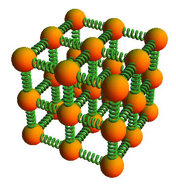
Figure 1. The lattice vibrations modeled as a classical mechanical system of balls and elastic springs.
By setting up the differential equations for such a system, we can see that the nuclear cores have kinetic energy and potential energy in three dimensions each. According to classical Boltzmann statistics, each degree of freedom should correspond to an average energy of ½ kT, where k is the Boltzmann constant and T is the temperature, defined in terms of Kelvin.
We consider each atom as a three-dimensional harmonic oscillator. The oscillator has kinetic energy and potential energy at the same time, and such a three-dimensional oscillator should therefore provide 2 * 3 degrees of freedom. In total, each atom should therefore provide an average thermal energy of 2 * 3 * ½ kT = 3kT. The free electrons, on the contrary, which only have the three dimensions of kinetic energy, and no dimensions of potential energy, should only provide 1 * 3 * ½ kT = 3/2 kT.
For one mole of a material, the heat capacity should therefore become Avogadros number, N, multiplied with the kinetic energy contributions from both the atoms and the electrons. The heat capacity of one mole should therefore sum up to N*(3kT + 3/2kT).
But instead of this, all observations showed that the heat capacity was much lower than N*(3kT + 3/2kT) at low temperatures – and stabilizing at around N*3kT at high temperatures.What was the reason behind the temperature dependency of the heat capacity, and why was there no significant contribution from the electrons?
We obtain the answer by substituting the classical harmonic oscillator representation of the nuclear cores with a quantum representation. The lattice vibrations are now modeled like a sum of so-called “eigen modes”, where each mode is a quantum harmonic oscillator. The quantum harmonic oscillators have energy of n*h*w0, where w0 is the frequency of the individual eigen mode and h is the Planck constant. The number n is an integer, and this integer tells us how many “phonons” there are in each eigen mode.
A phonon is a quasi particle serving to quantize the energy in the lattice vibrations. Within quantum mechanics, the phonons belong to the bosons, i.e. particles which have an integer spin and do not follow the Pauli exclusion principle. While the molecules of a gas follow the Boltzman distribution, the bosons follow the so-called Bose-Einstein distribution. For the Bose-Einstein distribution, a critical temperature must be reached before a linear dependency is established between the temperature and the number of phonons in the different eigen modes (the critical temperature is material-dependent).
Using the Bose-Einstein statistics, we can finally explain why some of the “degrees of freedom” are frozen out at low temperatures. Figure 2 gives an example of electrons and phonons interacting inside of the crystal lattice.
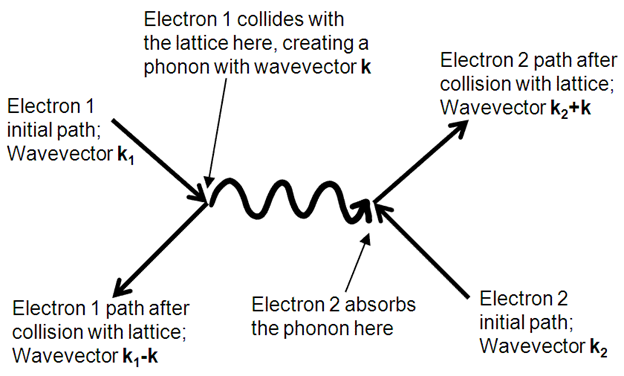
Figure 2. Example of interaction between phonons and electrons in the crystal lattice.
When it comes to the electrons, there is another principle – already briefly mentioned – that has to be introduced: The Pauli exclusion principle. It states that there can be no more that two fermions for each quantum state (and electrons are fermions). Unlike the bosons, which will all be packed together in the ground state when the temperature reaches zero, the electrons must be arranged, two by two, in the lowest available energy states.
At moderate temperatures, the Fermi energy (the highest energy the electrons may have at a temperature of zero degrees Kelvin) is much higher than kT. This means that only the electrons at states that are close to the Fermi level will obtain a thermal energy that is sufficiently high for jumping up to an unoccupied state. The rest of the electrons will remain at their zero degree ground states. There are just a few electrons that are thermally excited at moderate temperatures. This is contrary to the phonons which are bosons that do not obey the Pauli principle – and where every single phonon may be thermally excited from very small amounts of thermal energy. Because of this, the heat capacity at moderate temperature is dominated by the phonons – and and the electron contribution to the heat capacity at moderate temperatures is therefore negligible.
Electroncs – from particles to waves
With the Schrödinger equation for a free electron, a particle is modeled as a complex wave function. The time independent Schrödinger equation is written as:
E * Ψ = H * Ψ,
where Ψ is wavefunction, E is the energy of the wave, and H is the Hamiltonian function of the system.
The square of the wave function can be interpreted as the probability density function of the particle. If we modify the wave function in such a way that the particle is flying above a periodic potential, given by the attraction forces of the nuclear cores in the material, then we get a more realistic model for the electrons inside of a lattice structure.
We can do this by modulating the period potential into the wave function. Such a wave function is called a Bloch function. The Bloch function is written as:
![]()
where r is the position in the crystal lattice, k is the wavenumber, and u(r) is a function with the same spatial periodicity as the lattice.
By replacing the general wave function with the a Bloch function and solving the Schrödinger equation, we can extract a number of energy intervals that the electron is allowed to be within. Then it becomes clear that there are certain energies where no wave-like solutions exist for the particle. The electrons become located in certain “bands”, with forbidden energy gaps between the bands. On top of the energy gap, we have a so-called “conduction band” and on the bottom of the gap we have a so-called “valence band”.
When the band structure has come into place, it is easy to explain the difference in electrical conductivity between the different materials (See Figure 3):
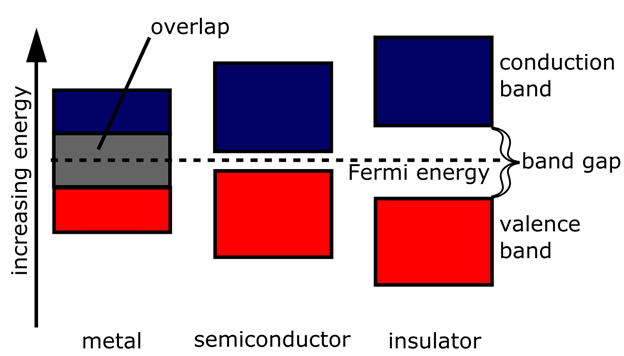
Figure 3. Metals, semiconductors and insulators are distinguished from each others by their band structures.
In a metal, the valence band has not been completely filled up with electrons, or valence band and conduction band have overlapping energies. Very little energy is therefore required to move an electron from one place in the valence band to another – or from the valence band to the conduction band.
In an isolator or a semiconductor, the entire valence band is filled up with electrons. This can only happen if the number of valence electrons per atom is an integer (as the Pauli principle only allows two electron per quantum state). If the energy gap up to the conduction band is high, the material becomes an isolator. If the gap is narrow, some of the electrons can obtain sufficient thermal energy to jump into the conduction band and become a conducting electron, just like in a metal. These materials, we call semiconductors.
We have to distinguish between direct semiconductors and indirect semiconductors. The difference is given by their band structure. In a direct semiconductor, the band structure is symmetrical around the energy axis, with the smallest band gap between band edges of the same wave number. A photon may therefore directly create an electron-hole-pair where the electron and the hole have opposite wave number. In an indirect semiconductor, like Silisium or Germanium, the smallest energy gap is between band edges at different wave numbers. An electron-hole pair can therefore only be created by also creating a phonon to conserve momentum. See Figure 4.
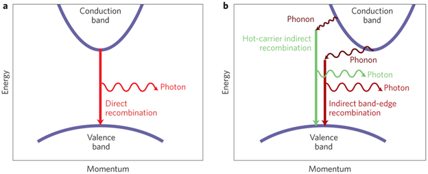
Figure 4. Difference between direct (left) and indirect (right) semiconductors.
Doping and PN Junctions
By introducing impurities into a lattice structure in a controlled way, we can fundamentally change the electrical properties of the material. This technique is called doping and the introduced impurities are called dopants.
All atoms strive to obtain a noble gas structure, i. e. to have eight electrons in the outer electron shell. In a silicon crystal structure, each of the four valence electrons in an atom make a covalent bond to an electron of a neighbouring atom. Like that, the desired noble gas structure is obtained for all the atoms in the lattice. However, if a dopant atom with five valence electrons is introduced into the structure, only four out of the five electrons will engage in covalent bindings with its neigbours and the last electron will remain a loosely bound electron. Such an impurity atom is called an N-type dopant.
The loosely bond electron of the N-type impurity atom becomes a localized impurity state, located right below the conduction band – to which it is easily thermally excited and can start moving freely around similar to a free particle.
Similarly, introducing an impurity atom with only three valence electrons will prevent a neighbouring atom from obtaining the desired noble gas structure – since only three out of its four valence electrons may form covalent bonds. Such an impurity atom is called a P-type dopant. The missing electron becomes a “hole” which can be filled – and hence move around in the lattice – when an electron belonging to a neighbouring covalent bond comes and takes its place.
Similarly to the loosely bound electron of the N-type dopant, the “hole” of the P-type dopant becomes a localized impurity state, but this time it will be located right above the valence band. An electron in the valence band can now easily be excited into this localized state, leaving a vacancy in the valence band. This vacancy can now move around in the valence band, similar to a free electron in the conduction band.
For an undoped semiconductor, the Fermi level of the material – also called the chemical potential – is located in the middle of the band gap. Introducing dopants into the material means shifting its chemical potential towards the impurity states. When N-doped and P-doped materials are joined, the two different chemical potentials must be aligned, and this gives rise to a “band bending” throughout the P-N junction between the materials. A contact potential between the P and N side is thus established, preventing charges from diffusing from one side to the other. See Figure 5.
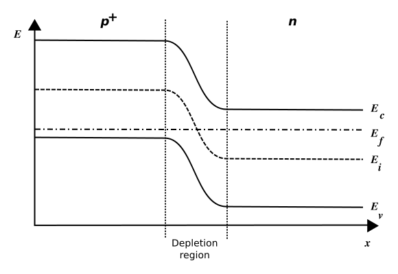
Figure 5. Alignment of Fermi levels across a PN junction.
By applying an external voltage on the P- and N-side, the shape of the barrier can be modified. Depending on the polarity of the voltage, the barrier can either be increased, i.e. widening the depletion region in the junctions, or it can be narrowed down and hence allowing the diffusion current to pass through the junction. The PN diode hence acts as a current rectifier.
Tunnel diodes
According to classical physics, a free particle will always bounce back when it hits a barrier with a potential energy higher than the kinetic energy of the particle. However, in quantum physics, there is a probability that the particle will “tunnel” through the barrier and continue moving as a free particle on the other side of the barrier. The probability depends strongly on the height and width of the barrier. Tunnel diodes take advantage of this effect.
With only a lightly doped silicon substrate, the wavelengths of the impurity holes and electrons do not overlap each others, and the impurities remain localized and are therefore allowed to have the same energy levels. With a heavily doped substrate, the impurity states start overlapping each others, and they are therefore forced by the Pauli principle to become part of the band structure. When heavily doped N-type and P-type materials are joined, the upper part of the P-side valence band will now overlap with the lower part of the N-side conduction band. The heavy doping also leads to a very narrow depletion zone of only a few nanometer. This means that a small forward bias may allow charges to tunnel through the depletion zone and recombine. However, as the voltage continues to increase, the overlapping regions will start shrinking and the tunnelling recombination current will start decreasing. The tunnel diode will therefore act as a negative resistor in a certain voltage range. This makes the tunnel diode excellent for implementing high frequency oscillators and switching circuits with hysteresis. See Figure 6.
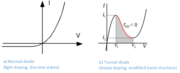
Figure 6. Characteristics of a normal diode (left), compared to a tunnel diode (right).
EEPROM and Flash Technology
EEPROM and Flash technology are other inventions which takes direct advantage of the tunnel effect. In normal NMOS transistors, a voltage is applied on the gate with the purpose of raising the surface potential of the substrate beneath the gate to a level where it exceeds the fermi level and becomes a conductive channel. However, instead of using a normal NMOS transistor with one single gate, a dual-gate transistor is introduced, with the second gate floating between the first gate and the NMOS channel. A high voltage is applied on the first gate, creating an electric field that is strong enough to cause tunneling through the silicon oxide, with electrons passing from the NMOS channel onto the floating gate. When the high voltage is turned off, the accumulated charges remain trapped within the floating gate, right above the NMOS channel – shielding the channel from the voltage applied on the normal gate and therefore keeping the transistor permanently turned off.
A programmed floating-gate transistor is comparable to a fuse that has been burned off and it can therefore be used for permanently storing information. The accumulated electrons on the floating gate can eventually be removed from by applying a reversed high voltage – making such circuits eraseable, and hence reprogrammable.
Light emitting diodes
Silicon is an indirect semiconductor. The energy released through the recombination of electrons and holes is therefore used to create phonons to conserve momentum. The recombination energy therefore gets lost in lattice vibrations.
In direct semiconductors, like Gallium and Arsen, can electrons and hole recombine with all the energy going into one single photon. A forward biased P-N junction will therefore emit photons of energy corresponding to the bandgap of the semiconductor.
Quantum dot lasers and quantum computing
For a totally free particle, the energy range is continuous – since all possible energies are allowed. For a particle flying above a periode potential, we have already seen that a band structure is implied, where certain energies are forbidden. But there is more to it than that: If we assume that the particle is not completely free, but rather confined within a certain volume, then the allowed energies are discretized into the energies of the standing waves that can be created within the box when the probability of finding the particle outside of the box becomes zero. Figure 7 shows examples of standing waves for a particle within a potential well, with the different harmonics corresponding to different energy levels.
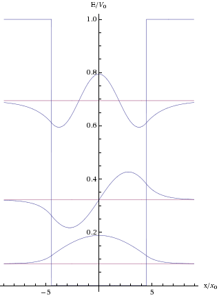
Figure 7. Examples of standing waves for a particle trapped within a potential well. The waves are in the middle with the boundaries of the well to the left and the right. Due to the tunnelling effect, the waves are able to extend into the “walls” of the potential well.
By creating patterns of P- and N-doped structures, junctions are created where the already explained band bending causes potential wells to establish. As the electrons and holes lose energy due to interaction with phonons (the quantized lattice vibrations), they might get trapped within the boundaries of the potential wells. Their energies will be discretized due to the structure of the potential well, and they will continue to lose energy until they are located in the lowest available energy levels.
A quantum dot is a potential well where the allowed energy is confined in all three dimensions – i.e. the height, width and length of the potential well is shorter than the De Broglie wavelength of an electron. The available standing wave energies in such a quantum dot will depend strongly on the shape of the quantum dot. Also the band gap energy of the quantum dot will be narrowed down, as the energy on the edges of the valence band and the conduction band will spread out into a number of discretized states. For such quantum dots, it can be shown that the highest density of available energy states lies around the ground state energies. The more compact the dot becomes, the more concentrated are the available states. See Figure 8.
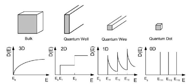
Figure 8. Schematic diagram illustrating the representation of the electronic density of states depending on dimensionality.
If the quantum dot is implemented in a direct semiconductor, like Gallium or Arsen, the trapped photons and electrons will localize in the ground states and emit photons of well-controlled wavelengths when recombining.A lot of research efforts are currently put into developing compact and controlled quantum dots. Recently, laser devices based on quantum dots are finding commercial applications within medicine, display technologies, spectroscopy and telecommunications.
Although still only on the theoretical stage, quantum dots are also promising for the future technology of quantum computing. In quantum computing, the different states of a particles in a potential well is used for encoding data. Instead of coding a zero or a one, the wavefunction of individual electrons can be used to code several bits.
Conclusion
Moore’s law has remained valid throughout the last decades. Transistor scaling has reached a level where transistor lengths of 14 nanometer has become normal – and the efforts continue for reaching even smaller dimensions. With transistor lengths reaching the wavelength of ionizing radiation, the art of electronics engineering becomes the art of quantum mechanical engineering. The quantum mechanical effects provide a lot of new challenges to overcome – like ever-increasing leakage currents due to tunnel effects – but the solutions also give rise to new and advanced technologies. The ones mentioned in this article are just a few examples of well-established technologies. Even more sophisticated technologies, like quantum computing, has been theoretically described already decades ago. The adventure of quantum electronics has just begun, so we will surely see even more inventions as soon as the processing technology becomes more mature.
Olav Torheim,
PhD in Microelectronics
Nye kommentarar